Review – SSD Memblaze PBlaze6 6530 3.84TB – Another great Gen4 solution at great price!
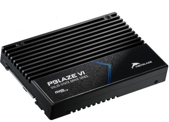
Today, we will be testing a high-end Datacenter NVMe SSD from Memblaze, the PBlaze6 6530 model, which is one of the most cost-effective SSDs offered by Memblaze.
It comes in a unique form factor called U.2, which resembles the well-known and older 2.5″ SATA connector. However, it features a 64Gbps bus, which means 4 PCIe 4.0 lanes, NVMe 1.4 protocol, and capacities ranging from 1.92TB to 7.68TB. As it has been on the market for some time, its average price on Alibaba is around $741 (for the 7.68TB unit), with the 3.84TB model estimated to be about half that price. This puts it in the same price range as a high-end consumer SSD, which is incredible!
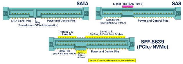
It’s interesting to note that Memblaze offers this lineup of SSDs in multiple form factors to meet the needs of data centers and servers. We received the SSD in the U.2 format, which, as we will see below, is quite similar to SATA. However, they also offer this lineup in other formats such as HHHL AIC, 2.5″ U.2, and E1.S.
We can observe that the pin-out of these connectors is quite different, as SATA uses 2 connectors while U.2 uses only 1. Additionally, the SATA connector uses the AHCI protocol to communicate with the host, whereas this SSD uses the NVMe 1.2 protocol with a PCIe 5.0 x4 bus to communicate with the host.
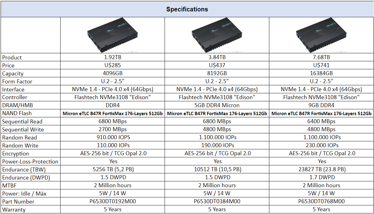
Specifications: MEMBLAZE PBlaze6 6530 3.84TB
Here are some more detailed specifications about the SSD that will be tested (3.84TB unit):
SSD’s Software
Unfortunately, we were unable to find software from Memblaze.
Unboxing
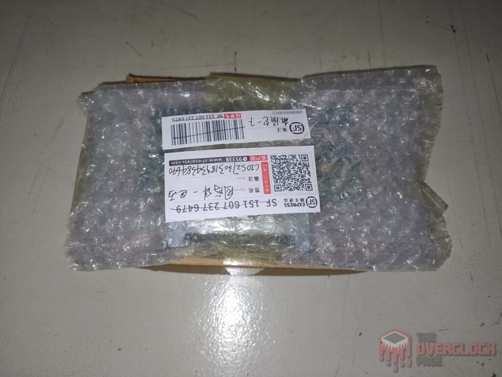
As this is a data center SSD, it arrived in a plain box, unlike consumer market products, which often come in detailed and flashy packaging.
It came in a brown cardboard box, and upon opening the box, we found the SSD secured in a styrofoam holder to keep it stable during transportation.

Its layout is very similar to the design of the other SSD Memblaze we tested previously.
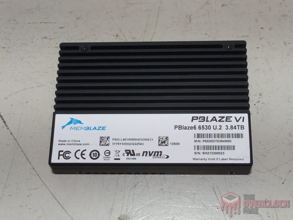
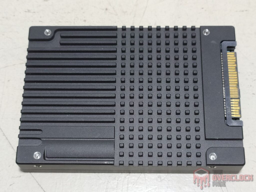
On the front, there is only a white label containing the SSD’s name and model, along with information such as its serial number and part number. On the back, we have an elegant design all in black. Still on the back, in the upper right corner, there’s a more rounded shape that indicates the presence of an electrolytic capacitor inside the SSD to provide Power-Loss-Protection.
An interesting point is that Memblaze recently had a patent approved for this case design, as seen in the image below.
On the side, it has a connector for debugging that allows data collection through UART and JTAG.
Upon opening the SSD, as shown in the image below, we can see that it is secured by four star-shaped screws, commonly known as Torx T6.
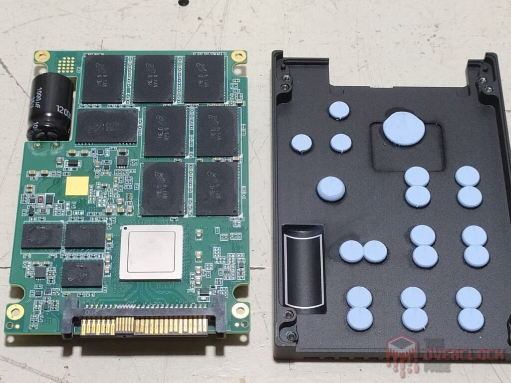
Upon removing the screws and the top casing, we encounter the build quality and attention to detail of the SSD. Its rear casing has a metal plate that aids in heat dissipation, and the entire back of the PCB is covered with 1mm thermal pads.

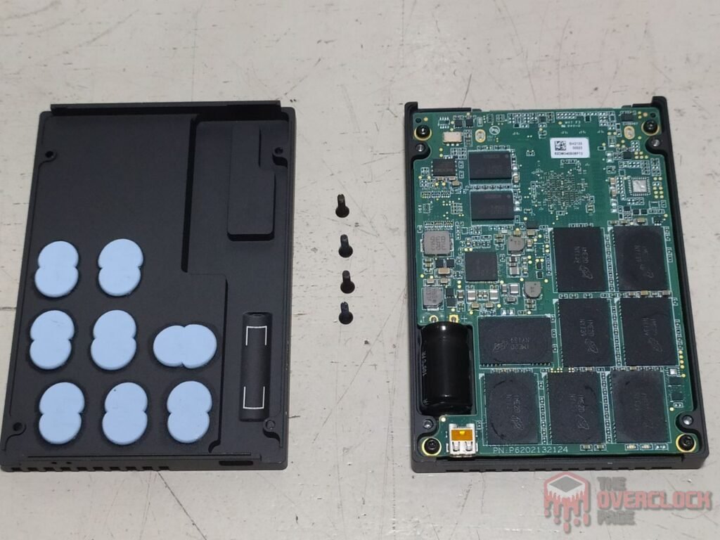
To open the rest of the SSD from the top casing, we need to remove four more Torx-T6 screws that secure the PCB.
By default, it comes with 14.5% allocated for over-provisioning. On its front PCB, we find numerous chips, including the controller, 8 NAND flashes, and 3 DRAM Cache modules, as well as several VRM and PLP ICs.

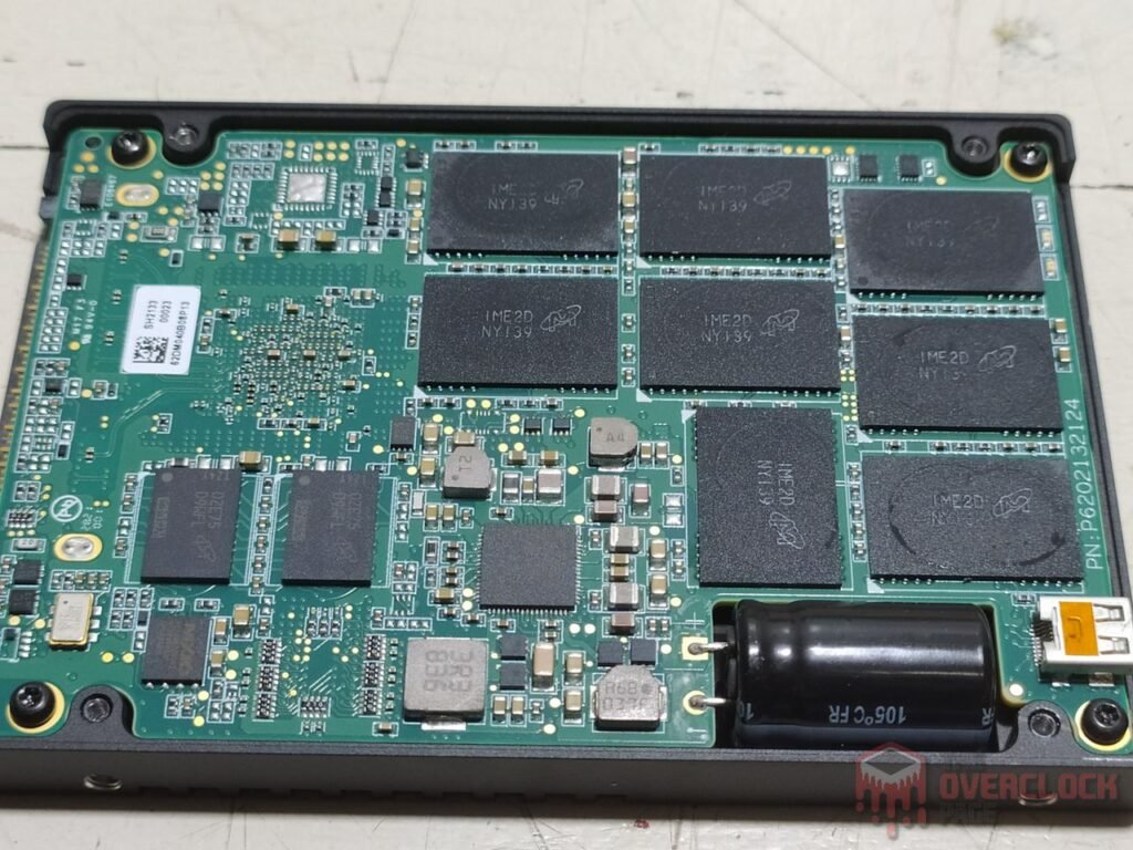
On the back side, there are 8 more NAND Flash modules and 2 DRAM Cache modules.
Controller
The SSD controller is responsible for managing all data, over-provisioning, and garbage collection, among other background functions. Naturally, this contributes to the SSD’s good performance.
Datacenter SSDs typically do not use the controllers we see in consumer market SSDs. Therefore, we won’t see controllers like the Phison E18 or other controllers such as the Silicon Motion SM2264.
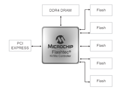
In this SSD, Memblaze uses a controller from FlashTech Microchip, nicknamed “Edison” NVMe3108.
Being a Datacenter controller, it includes certain features that we don’t typically see in other consumer market SSD controllers.
This lineup of controllers has two variants: the NVMe3108, which offers 8 communication channels, and the NVMe3016, which has 16 channels. In this SSD, the NVMe3108 is employed.
This controller features a 64-bit ARM architecture with 6 Cortex-A53 cores (Hexa-core) for main data processing and NAND Flash management. For those more attentive, you might recognize these Cortex-A53 cores, as they are widely used in smartphones and tablets. In mobile devices, we typically see between 4-6 cores operating at frequencies above 2GHz; here, they are likely running at lower speeds for greater power efficiency.
In addition to the Cortex-A53 cores, the NVMe3108 also utilizes two other types of architecture, the CoreLink™ CCN-502 and the GIC-500. These are not regular processing cores like the Cortex-A53; instead, they are specialized components for interconnection and interrupt management, respectively. They enhance the performance, scalability, and efficiency of multi-core systems, such as the U.2 SSD with the NVMe3108 controller that we are testing.
It also supports DDR4-2400 MT/s DRAM Cache with a 72-bit DDR interface (64-data + 8 ECC) and up to 128GB of DRAM.
Its 8 channels have an NV-DDR4 bus of 1200 MT/s (600 MHz), which isn’t as fast as the Phison E18 controller. However, one of the main differentiators is that it supports interleaving up to 16 Chip Enables per channel, allowing this controller to directly communicate with up to 128 dies. This capability is uncommon in consumer SSD controllers.
Most high-end consumer segment controllers, such as the Phison E18 and Phison E26, typically support up to 32 dies (8 channels and 4 Chip Enables per channel). In contrast, this FlashTech controller offers 8 channels and 16 Chip Enables per channel.
DRAM Cache or H.M.B.
Every high-end SSD that aims to offer consistent high performance needs a buffer to store its mapping tables (Flash Translation Layer or Look-up table). This allows it to achieve better random performance and be more responsive.
Datacenter SSDs also use a significant amount of DRAM Cache for mapping tables, but they don’t always follow the common 1:1000 ratio seen in consumer market SSDs, where we typically see 1GB of DRAM Cache per 1TB of storage.
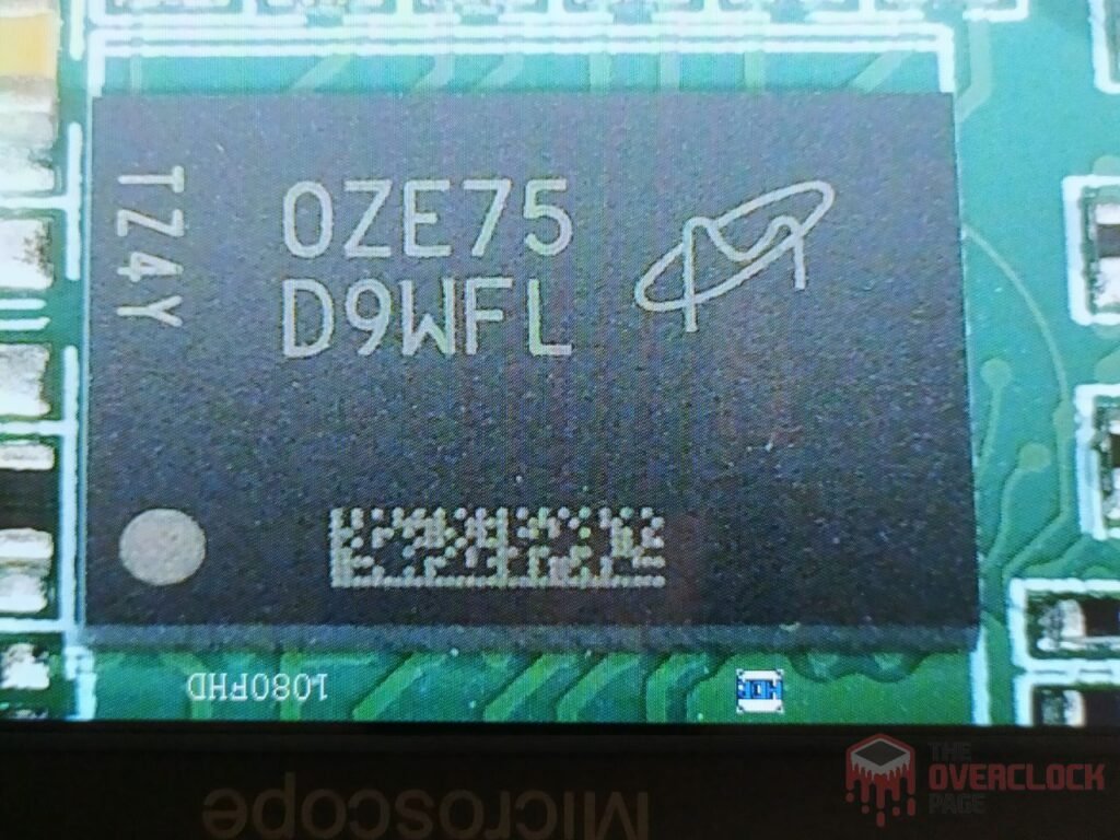
On its front PCB, near the controller, you can find 3 DRAM Cache modules from the American manufacturer Micron, model “D9WFL“. Using Micron’s decoder, this translates to “MT40A1G8SA-062E“, which are DDR4-3200 MT/s modules with 8Gb (1GB) density each, operating with CAS-22 latency. Therefore, on its front PCB, it has 3GB of DRAM Cache.
On its rear PCB, the SSD has an additional 2 modules, also from Micron and of the same model, D9WFL, providing another 2GB of DDR4.
In total, this SSD has 5GB of DDR4-3200 MT/s CL-22 DRAM Cache. However, 4GB is likely used for storing the Flash Translation Layer (FTL), while the remaining 1GB is probably used for ECC (Error Correction Code) as redundancy.
NAND Flash
Regarding its storage integrated circuits, the 3.84TB SSD has 16 NAND flash chips marked as “NY139“. Using the manufacturer’s decoder, we identify the NANDs as “MT29F2T08EMLEEJ4-T:E“. These are NANDs from the American manufacturer Micron, model B47R FortisMax. In this case, the dies are 512Gb (64GB) each, containing 176 layers of data and a total of 195 gates, resulting in an array efficiency of 90.2%. Of the 195 layers in the SSD, 176 are allocated for storage, contributing to this efficiency.


The B58R dies are of the eTLC (Enterprise Triple-Level Cell) type, but what are eTLC and how do they differ from traditional TLC chips?
It’s important to note that NAND Flash chips come in various durability categories, with different manufacturers categorizing their wafers accordingly. This SSD uses Micron’s FortisMax chips, which offer greater endurance than those in consumer SSDs. However, they are more expensive due to their selection from higher-quality wafers.
We have the FortisFlash, which are the most famous and commonly used in consumer SSDs. We have the MediaGrade, which is typically seen in QLC dies and tends to have slightly lower durability compared to FortisFlash.
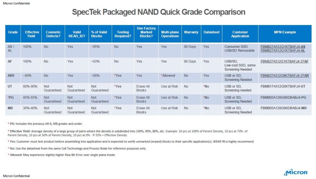
And finally, we have SpecTek. Spectek is a subsidiary of Micron that uses DRAM chips and NANDs that sometimes don’t go through all of Micron’s endurance and quality control tests and are resold under the SpecTek brand as more affordable options. They tend to have lower durability.
However, these SpecTek dies also have durability classifications and recommended use, as shown in the image below.
In this SSD, each NAND Flash chip has 4 dies with a density of 512Gb, totaling 256GB per NAND chip. With 16 NAND chips in total, this results in a capacity of 4TB. They communicate with the controller via a 1200 MT/s bus, which is unfortunately well below the 1600 MT/s they are capable of delivering, due to the controller’s limitation.
PMIC (Power Delivery)
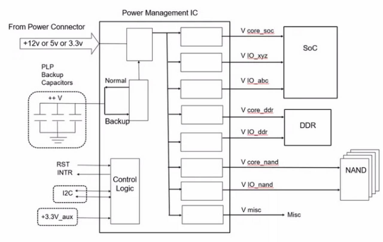
Like any electronic component that performs work, SSDs also have a power consumption level that can range from a few milliwatts to nearly 25 watts, close to the limits of some connectors or slots. The circuit responsible for all power management is the PMIC, which stands for “Power Management IC,” a chip responsible for supplying power to other components.

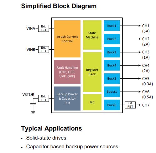
We can see that the main IC of this SSD is a PMIC from Integrated Device Technology (IDT), model IDT P8330-5M2, which is a subsidiary of Renesas. It’s clear that this IC is a single or multichannel SSD Power Management Solution.
As we can see in the block diagram above, it can handle up to 6 step-down regulators with internal MOSFETs, with each one having a current level and voltage in each channel. It’s specifically designed to work in SSDs, and it offers various protection systems such as overcurrent, overvoltage, undervoltage, undercurrent, overtemperature, among others.
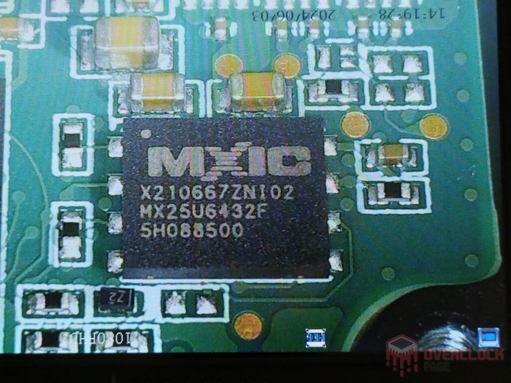
Another IC found in this SSD is marked as “MXIC MX25U6432F” from the manufacturer Macronix. This is a NOR flash memory chip, commonly found in computer and laptop motherboards to store the BIOS (firmware) of the boards.
In a datacenter SSD like this one, the manufacturer might have chosen to use this circuit to store the SSD’s firmware directly or for other purposes such as storing Bootloader information. The Bootloader is a small program that initializes the SSD’s hardware and loads the firmware into the controller’s memory right after the P.O.S.T. (Power-On Self-Test).
It could also be used to store essential configuration data for managing the NAND Flash, including certain parameters for the controller. Another key point is that it might be employed for security purposes, ensuring that only authentic firmware is loaded onto the SSD by performing authentication during startup.
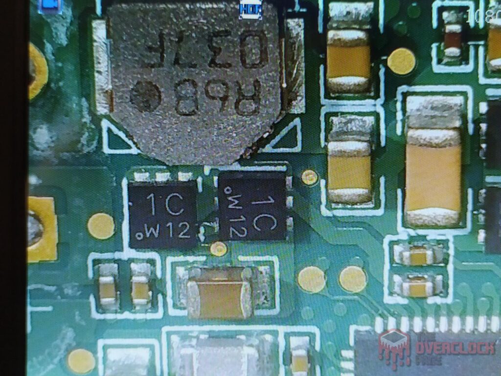
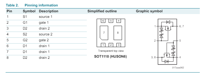
We also have another IC marked as “1C W12,” which belongs to NXP Semiconductors. This is a dual-channel P-Channel MOSFET, model “PMDPB65UP,” which supports operating up to 20V, 3.5A, and has a thermal working capacity of up to 150ºC. It also features a thermal resistivity of 1.25ºC/W (ambient) and 8.3ºC/W for the package, which is quite high.
Power-Loss-Protection
Power Loss Protection in Datacenter SSDs is crucial to ensure data integrity during power failures. By using capacitors or temporary energy storage, it enables the safe completion of ongoing operations, preventing data corruption in critical environments. This ensures high data availability and reliability.
In this drive, we can see that it has a huge electrolytic capacitor from the manufacturer Nichicon, which produces various integrated circuits like this. Nichicon is a Japanese manufacturer and is one of the best capacitor manufacturers in the world.


This electrolytic capacitor can operate with voltages up to 35V and has a capacitance of 1000?F. It is rated to temperatures up to 105ºC.
SSD Power States
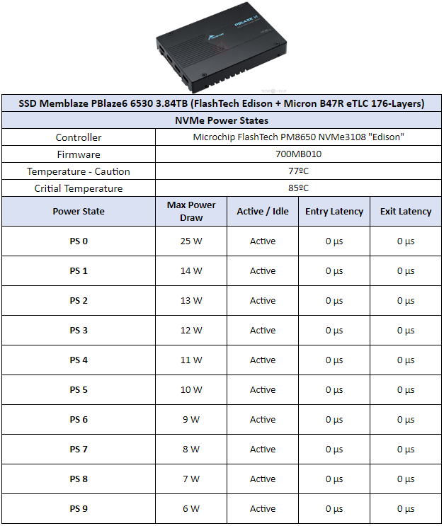
As mentioned in previous sections regarding power consumption, in this segment, we will delve further into the power states of this SSD.
Something peculiar about this unit is that typically SSDs have 5 primary power states, but in this case, we see that it has 10 active power states ranging from 25W to 6W. In PS 9 at 6W, even though it is an active power state, it is considered a low workload state.
SSD MEMBLAZE PBLAZE6 6530
Just like integrated circuits on a RAM module can vary, the same can happen with SSDs, where there are cases of component changes like controllers and NAND flash chips.
Memblaze offers two versions of this product with two different segments, making a total of four options. We have the 6530 series with capacities of 1.92TB, 3.84TB, and 7.68TB, which offer an over-provisioning volume of 14.5%.
There are also other models marked as 6536, which have slightly higher performance with capacities of 1.6TB, 3.2TB, and 6.4TB. These models offer an even larger over-provisioning volume of about 37.4%, and they also have greater durability with 3.3 DWPD (Drive Writes Per Day) compared to the 1.5 DWPD of the 6530 series.
TEST BENCH
– Operating System: Windows Server 2019 64-bit (Build: 22H2)
– CPU: Intel Core i7-13700K (8C/8T) – All Core 5.7GHz – (Hyper-threading and E-cores disabled)
– RAM: 2 × 16 GB DDR4-3200MHz CL-16 Netac (w/ XMP)
– Motherboard: MSI PRO Z790-P WIFI DDR4 (Bios Rev: 7E06v18)
– GPU: Raptor Lake UHD Graphics 770
– SSD (OS): SSD IronWolf 125 1TB (Firmware: SU3SC011)
– SSD DUT: SSD Memblaze Pblaze6 6530 3.84TB (Firmware: 0A1022T0)
– Intel Z790 Chipset driver: 10.1.19376.8374.
– Quarch PPM QTL1999 – Used for power measurement.
ADAPTORS
As it is a U.2 interface SSD, consumer PCs do not have the required interface to connect them, so an adapter from U.2 to PCIe is needed. In this case, you are using a PCIe 5.0 x4 NVMe adapter.


The only problem is finding adapters like this for SSDs as fast as the ones tested, because U.2 to PCIe 3.0 adapters are quite affordable, often under $50-$100. However, these Gen 5.0 adapters can cost more than $700, not including the SSD itself.
TESTING METHODOLOGY
Because this is a server-oriented SSD, it doesn’t make sense to test it using benchmarks intended for consumer drives. Instead, we will use our test suite for Datacenter/Enterprise SSDs.
Here’s the testing process:
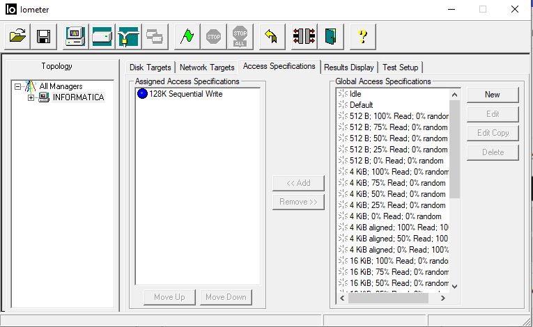
The software used is IOmeter 1.1.
- Multiple Secure Erase operations are performed at the end of each benchmark.
- To prepare the SSD, data is sequentially written to at least 2x the drive’s capacity before logging.
- Pre-conditioning of the SSD is performed with a high queue depth workload specific to each benchmark before logging.
- Once the SSD is ready, data is written for 5 minutes to monitor performance.
WHERE TO BUY
This SSD can be found directly on Alibaba’s official Memblaze store. Links are provided below:
IOmeter – Sequential and Random
Sequential: 128 KiB Blocks, 256 Queues, 1 Thread
Random: 4 KiB Blocks, 32 Queues, 1 Thread (100% Aligned – Write/Read)
Before measuring its speeds, the SSD needs to be “prepared” or preconditioned to ensure that the performance it offers is consistent. SSDs have three states: Fresh-out-of-Box (FOB), the Transitioning state, and the Steady State.
F.O.B. (Fresh-out-of-Box) represents the state when the SSD is first tested under any workload. The Transition state, as the name suggests, is the phase of change until it reaches the Steady State. The Steady State is the continuous performance state where the SSD’s performance remains constant under the workload and does not change, maintaining this state continuously.
A simple analogy to understand these three states would be this: Imagine you are a marathon runner. At the beginning of the race, you give your best, reaching your maximum speed. However, it is physically impossible to maintain this speed throughout the entire course. Let’s say at this peak moment at the start of the race, you manage to average 15 km/h. Maintaining this pace for the entire distance is impossible, so as you continue, you begin to lose speed.
This period when your speed starts to fluctuate would be the Transitioning state. However, once you begin to stabilize and run at a speed that you can maintain until the end of the race, that would be the Steady State.
IOmeter – Sequential
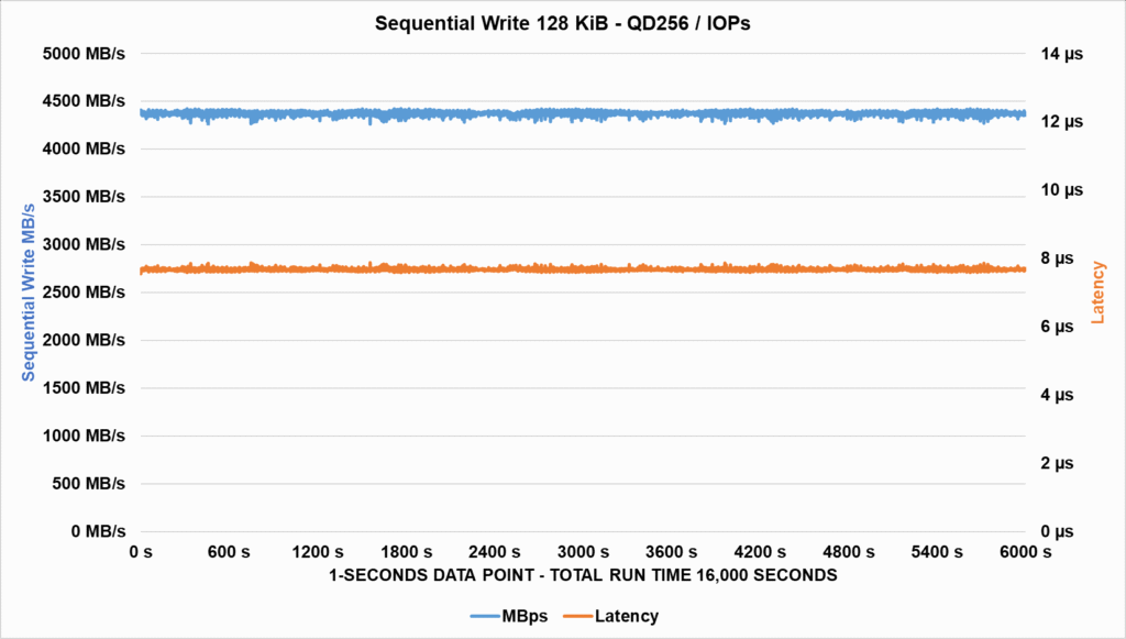
Starting with a sequential write test using 128 KiB blocks, we can observe that throughout the test, the speed is quite consistent. As mentioned, these types of SSDs do not feature SLC Cache. Additionally, their latencies also showed good results in this scenario.


Now testing its sequential speeds at multiple Queue depths, the SSD reaches speeds of over 4.5GB/s at QD4 – QD8 and maintains this up to QD256. At lower QD levels, such as 1 to 4, it ranges between 1.5GB/s and 2.8GB/s. There is a noticeable difference compared to the other Gen5 SSD we tested earlier.
Regarding latencies, we observed that it performed well for a Gen4 SSD. However, at higher QD levels, there was a significant increase in latencies, which was more moderate in the Gen5 SSD.
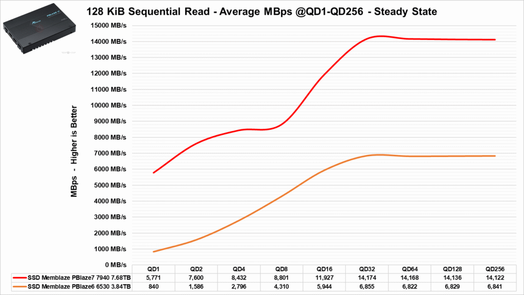
In terms of read speeds, it can achieve its nearly 7 GB/s described speeds only at QD levels of 32 and above, similar to the other Gen5 SSD. Below this, from 1 to 16, it ranges between 800 MB/s and 6 GB/s.
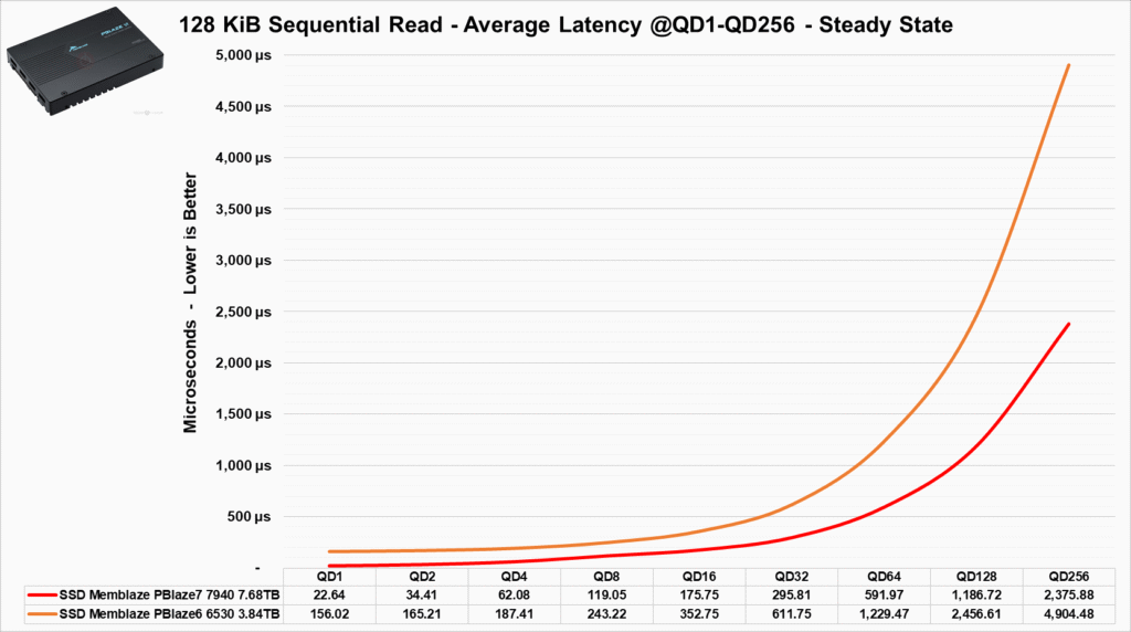
At least its latencies don’t become as high at large QDs (128 and beyond) as they do in writing, which is a better result.
IOmeter – Random 4 KiB
Let’s proceed with the preconditioning of the SSD to perform the 4 KiB benchmarks.
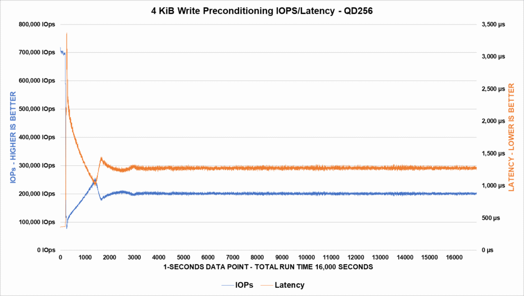
We can observe that the SSD starts writing at almost 700,000 IOPS in its FOB state. However, it quickly drops drastically and then starts to rise again until it stabilizes after 3000 seconds. This period is the Transition state, and from then until the end of the benchmark is the Steady State. It managed to stabilize slightly above the specified range, maintaining around 200,000 IOPS.
This is the same behavior observed with its latencies.
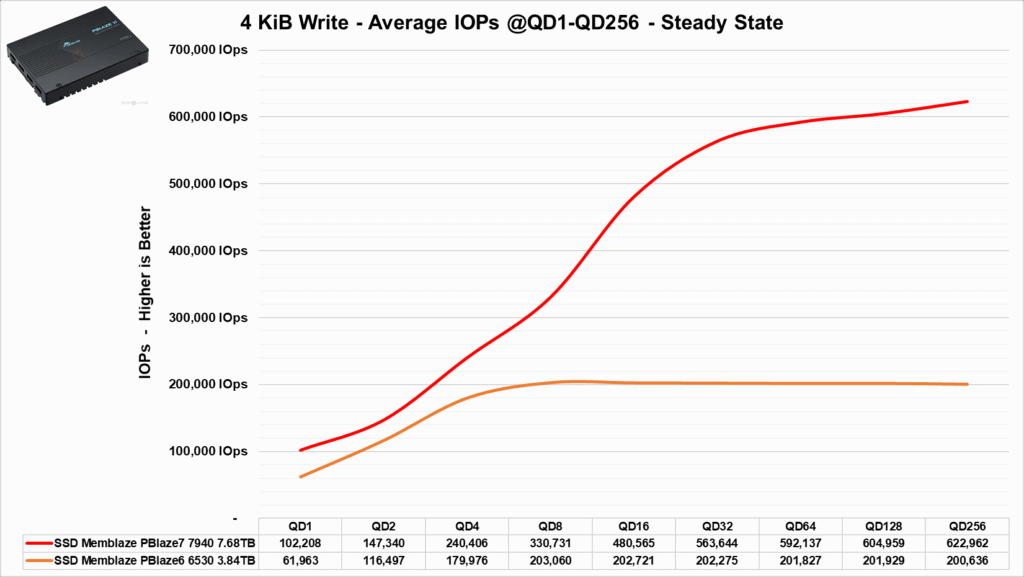
After completing the preconditioning, we proceed to the write test.
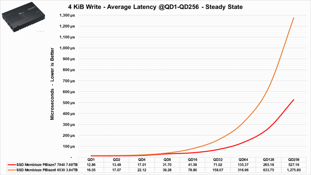
We can observe that the manufacturer rates this SSD at 190K IOPS for sustained write performance, and it already achieves this performance between QD4 and QD8, which is an excellent result. The Gen5 SSD, despite having a much higher rated performance, needs to exceed QD128 to deliver the promised performance.
In terms of latency, it shows very low latencies at QD1, although it was slightly higher than the specified 11µs, coming in at 16µs. This could be due to the testing platform used.
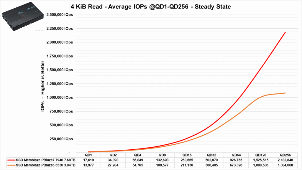

In its read performance, we see that it approaches 1.1 million IOPS, reaching the value specified by the manufacturer, but only at QD levels of 256 and above.
In terms of latency, the manufacturer specifies 72µs at QD1, and it indeed delivers as promised, with the difference not being very significant compared to the Gen5 SSD.
Benchmark: 4 KiB 70% Read 30% Write
One of the most commonly used metrics in SSD benchmarks represents multiple uses in various servers and data centers. In this benchmark, we will run the test for over 16,000 seconds to see how the SSD performs.
We can observe that the SSD starts strong with over 750,000 IOPS but then drops and stabilizes, reaching a Steady State at around 480,000 IOPS after approximately 5,000 seconds.
In terms of latency, it took the same amount of time to reach a steady state.
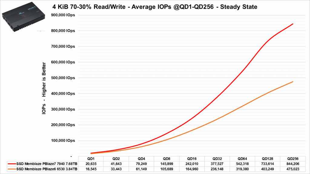

When comparing both Memblaze SSDs, we can see that there is indeed a difference between the two, especially at higher QDs. However, both exhibit excellent performance for their respective performance categories.
Random Write and Read 8 KiB
In this section of the benchmark, we will use 8 KiB blocks, which are commonly used in virtualized environments and OLTP (On-Line Transaction Processing) scenarios, frequently seen in banking operations, purchases, and similar applications.
During the 16,000 seconds of plotting, we see that the SSD, both in terms of latency and bandwidth (IOPS), reaches the steady state around 3,000 to 4,000 seconds. Subsequently, the SSD maintains an average performance of over 90K IOPS. Meanwhile, its latency stabilizes below 2800µs or 2.8ms.
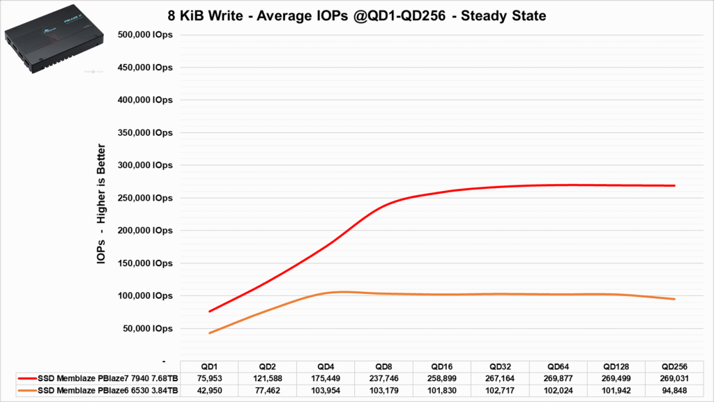

In terms of its bandwidth in IOPS, it starts with approximately 42K IOPS at QD1, compared to Gen5, which is almost twice as much. However, it increases as the QD count rises, stabilizing at QD4, where it reaches its peak performance. From QD4 to 256, the SSD remains close to 102K IOPS.
The same can be said for its latencies, as it presents excellent results even when compared to the Gen5 SSD.

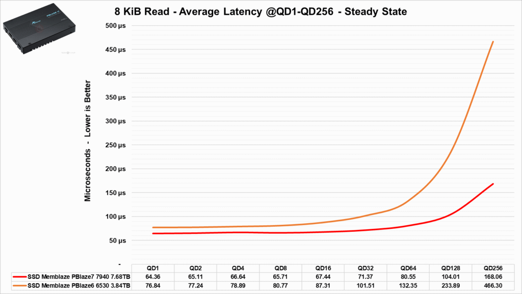
When analyzing its random read performance with 8KiB blocks, we can observe that up to QD8, even though it is a Gen4 SSD, it remains quite close to the other Memblaze Gen5. It only falls behind when exceeding QD16 and beyond. The same can be said for its latencies.
Benchmark: OLTP Server Workload
In this section of the benchmark, we will replicate a typical workload found in servers handling banking transactions or other online shopping environments that perform transactions and HFT (High-Frequency Trading). HFT is a financial trading strategy that involves buying and selling financial assets, such as stocks, bonds, currencies, and commodities, at high speed and with a large volume of operations.
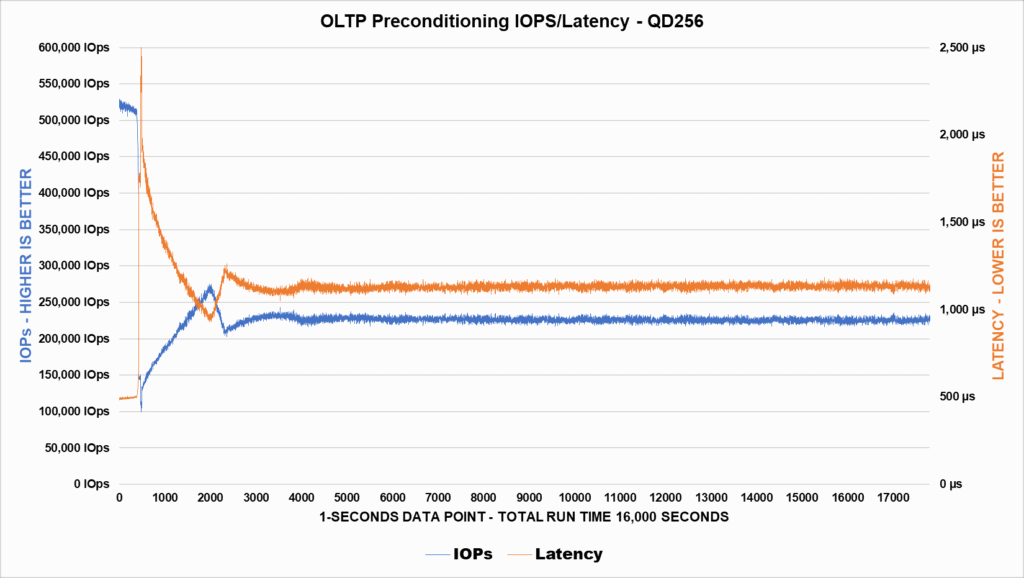
When performing the preconditioning of the SSD, we can see that it stabilizes (Steady State) after approximately 4,000 seconds into the benchmark. Its bandwidth stabilizes above 230K IOPS, while its latency stabilizes around 1200µs.
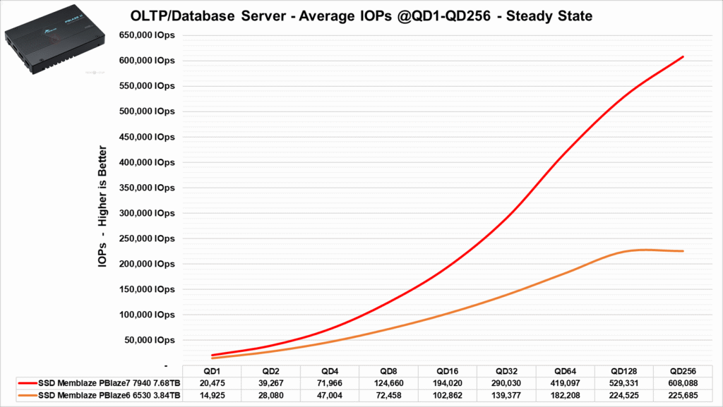

We can observe that it can deliver more than 220K IOPS at QD256 for larger servers with a high processing queue, while at lower QDs, it still provides good performance but is slightly inferior to the Gen5.
And even in terms of latency, it presents good results at lower QDs, being very close to the Gen5 SSD.
Benchmark: Web Server Workload
In this test, a typical load found in “web servers” was simulated, which often handle various file sizes and block sizes, ranging from 512 bytes to 512KB. Additionally, different types of access were tested, including Read and Write operations, as well as a mix of both in varying percentages.
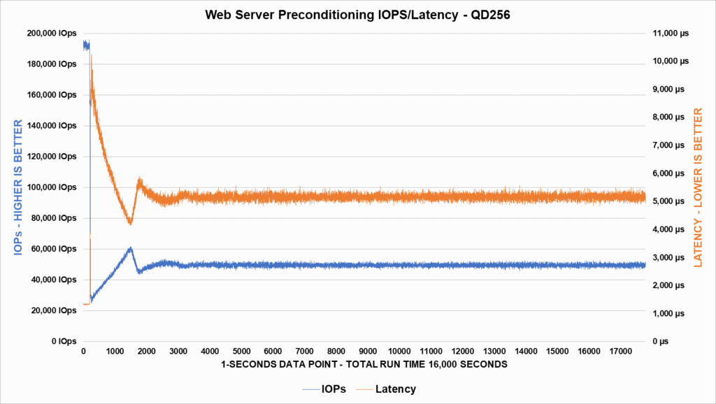
In this scenario, it takes approximately 3,000 seconds to reach Steady State, with its latencies stabilizing around 4.7ms and its bandwidth stabilizing around 50K IOPS.
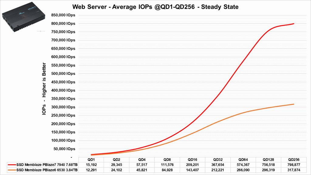
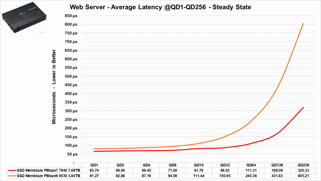
For this type of workload, this SSD has proven to be very capable, delivering almost 315K IOPS at QD256. Depending on the size of the email server, the workload might not exceed QD128, but even so, it still shows good results at lower QDs for a Gen4 SSD. Naturally, the Gen5 SSD surpasses it at very high QDs, but for servers with smaller workloads, the difference is imperceptible.
The same can be said about its latencies, which remain quite low at lower QDs, only increasing at higher QDs like 256, but still remaining comparable to the Gen5 SSD.
Benchmark: Email Server Workload
In this section of the analysis, we will use a typical workload found in email servers, which traditionally work with 8 KiB block sizes and a 50%/50% distribution (Random Read/Write). This scenario is also considered more demanding for write operations on the device.
We can observe that during this preparation, the SSD took a little over 3000 seconds to reach Steady State, where it maintained a consistent performance around 170K IOPS with latencies close to 1500µs.
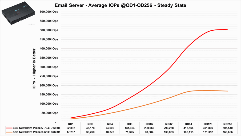

In this other benchmark, starting with its bandwidth, it achieves excellent results in small email servers, even when compared to the Gen5 SSD. The difference becomes more pronounced only at very high QDs, such as above QD32.
Its latencies were also quite similar to the Gen5 SSD at lower QDs, only increasing significantly as the QD count rose, particularly at QD128 and above, where they became more than three times higher than those of the Gen5 SSD.
Benchmark: Big Data Analytics Workload
In this section of our review, we will simulate a data load commonly found in this field. But what is BDA? Big Data Analytics is the process of examining and extracting valuable insights from massive and complex datasets to make informed decisions and improve business performance. We ran a sequential read test for 5 hours with 1 MiB blocks and 100% aligned sequential access.


We can observe that during most of the bandwidth test, especially at higher QDs, there was a significant difference compared to the Gen5 SSD. However, this difference should be smaller when compared to another Gen4 SSD.
In the latency test, although its latencies were on average twice as high as those of the Gen5 due to its lower bandwidth, it still achieved a satisfactory result.
Benchmark: Machine Learning (A.I.)
Machine Learning is a subfield of artificial intelligence that focuses on developing algorithms and models that enable systems to learn and improve from data without explicit programming. This approach allows machines to identify patterns, make predictions, and make decisions based on the acquired information, becoming a valuable tool in a variety of applications, from product recommendations to medical diagnoses.
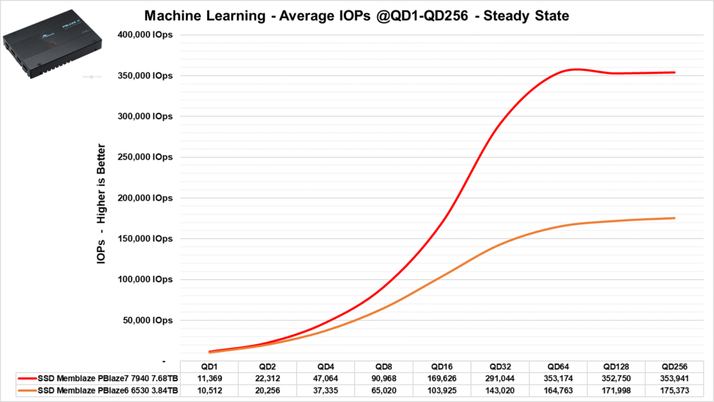

In this benchmark, where we used 32 KiB blocks in random read, we see that it reaches a peak of almost 175K IOPs at QD256, which is a satisfactory result. However, at lower QDs, its performance is almost identical to the Gen5 SSD.
The same can be said about its latencies, which only become noticeably higher at larger QDs.
TEMPERATURE STRESS TEST
In this section of the analysis, we will observe the temperature of the SSD during a stress test, where the SSD continuously receives files. This will help us determine if there is any thermal throttling with its internal components that could cause any bottleneck or performance loss.
As seen above, this SSD has a default thermal throttling limit of 77°C to 85°C, which is quite reasonable for an SSD of this category. However, during our battery of tests, it did not reach 70°C on its sensors, which meant the SSD did not experience thermal throttling at any point during the test. This is another impressive result.
POWER EFFICIENCY AND CONSUMPTION
SSDs, like various other components of our system, have a certain power consumption. The most efficient ones can perform requested tasks quickly and with relatively low power consumption, allowing them to transition back to their idle power states where they tend to consume less power.
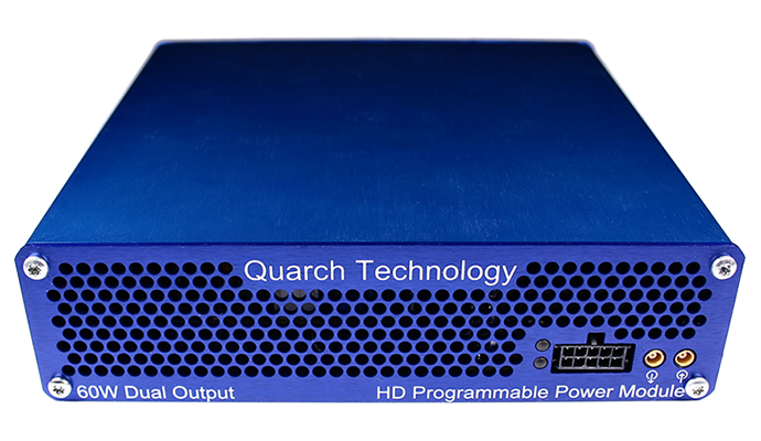
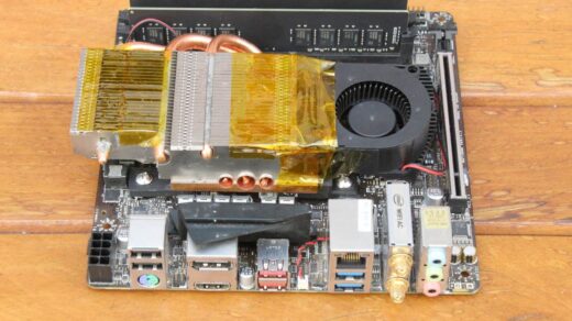
In this part of the analysis, we will use the Quarch Programmable Power Module, provided to us by Quarch Solutions (as shown in the photo above), to conduct these tests and assess the SSD’s efficiency. This methodology will involve three tests: the maximum power consumption of the SSD, an average in practical and casual scenarios, and the idle consumption.
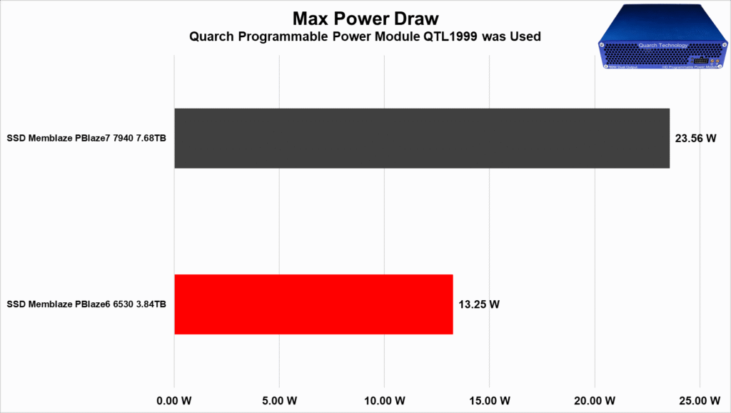
Although this SSD has its Power State 0 configured at 25W, it doesn’t even come close to that. In all the tests we conducted, we couldn’t find a consumption higher than 13.25W, which is an excellent result for an SSD like this. It was even 10W lower than the Gen5 SSD.
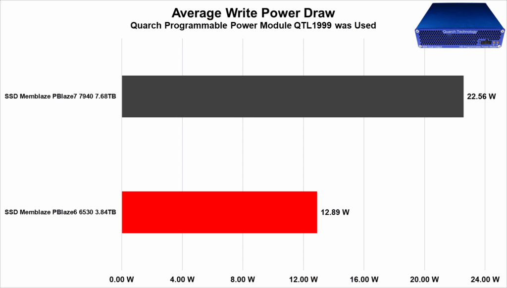

When conducting our SSD fill test, starting with its write performance, we observed an average power consumption of 12.89W during this benchmark. This was again almost 10W below the previously tested Gen5 SSD, while its bandwidth remained above 4500 MB/s.


In the read test, we observed that the SSD had very low power consumption, almost half compared to the write test, while its bandwidth remained high, exceeding 6900 MB/s.
Lastly and most importantly, let’s discuss the idle test, as this is the scenario in which the vast majority of SSDs are found in everyday or routine use. Although 4.41W for an M.2 SSD might seem like high “maximum” consumption, an enterprise data center SSD like this one tends to have much higher consumption due to the more robust controllers, numerous NAND Flash Dies, and DRAM Cache. Additionally, there are numerous capacitors and components for the VRM and the Power Loss Protection circuit.
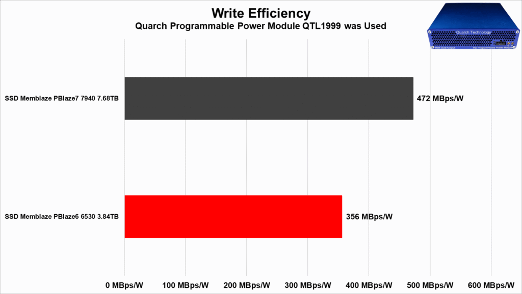
Regarding its efficiency, starting with writing, we see that although it had much lower power consumption than the Gen5 SSD, high efficiency is not achieved solely through low power consumption. A high bandwidth is also necessary.
As we see in this scenario, it falls behind the Gen5 SSD. Despite the Gen5 SSD having much higher power consumption, its bandwidth was more than twice as large, which contributes to its efficiency.
Not that the bandwidth of this SSD was poor; on the contrary, achieving nearly 5GB/s for enterprise SSDs of 4TB is quite impressive. The fact is that Gen5 SSDs, although consuming more power, have such high bandwidth that it somewhat “overlooks” this aspect.
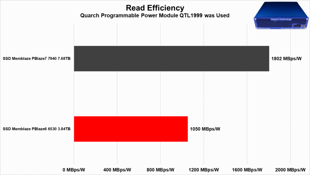
The same can be said for its read efficiencies. Although both have highly respectable speeds in this scenario and power consumption within market standards, the bandwidth creates this significant gap.
Conclusion
Taking everything into account, is it really worth investing in this SSD?
This SSD is not aimed at the consumer market but rather the corporate sector, specifically for use in data centers. Therefore, it is an excellent SSD for such applications, especially in web servers, OLTP, and other similar uses. Additionally, the cost per unit and per batch can be significantly lower than Gen5 SSDs while still delivering satisfactory performance.
ADVANTAGES
- Excellent Sequential Speeds: Exceeds 6,900 MB/s.
- Impressive Random Speeds: Can surpass 1.1 million IOPS in certain workloads.
- Outstanding Latencies: Depending on the workload.
- Data Center Performance: Excels in lower QD scenarios and in read operations.
- Solid Build Quality: Features a robust controller and excellent NAND Flash.
- Durability: On par with other products using similar NAND Flash.
- Versatile Form Factors: Available in formats suitable for servers, including U.2, AIC HHHL, and E1.S.
- No Thermal Throttling: Maintains performance under heavy use.
- Consistent Hardware: No variations in components.
- Enterprise Features: Supports AES-256 bit encryption and other enterprise-level features.
- Low Power Consumption: Very efficient in various scenarios.
- Excellent Energy Efficiency: Optimized for energy-saving.
- Aggressive Pricing: Competitive price point.
DISADVANTAGES
- Not Available in E3.S Form Factor: Limited form factor options.
- Lacks Management Software: No proprietary software for SSD management.
- Limited Warranty Coverage: 5-year warranty available only in China, not yet available in Brazil.
